Circuitry Architects
Situated at the intersection of chemistry, physics and chemical engineering, the semiconductor (microelectronics) industry enables a greener, smarter, and more connected economy. The field has significant implications in society’s ability to support technology innovations and address the global energy crisis through applications in microprocessors, photovoltaics, LEDs and power transistors. For students who love to stay connected, semiconductor technology has driven advancements in the internet, 5G and IoT (Internet of Things). And for the tech geeks who love smart technology – iPhone, Fitbit, self-driving cars- this field is ripe with opportunities. The continued success of this vast, interdisciplinary, and sophisticated yet innovative industry is deemed critical to long term US national competitiveness, which translates into impactful and well-paid job opportunities for those who choose to join this sector.
paid internships since 1998
compensation for offers in past year
within three months
What are semiconductors?
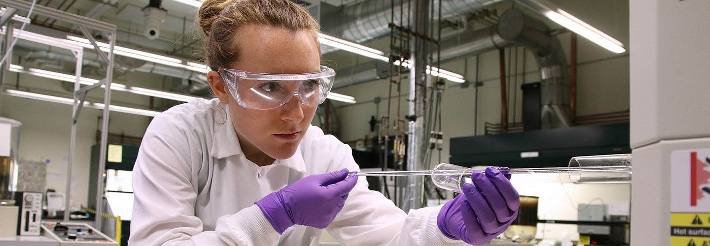
Semiconductors are an essential component of electronic devices, enabling advances in communications, computing, healthcare, military systems, transportation, clean energy, and countless other applications.
For the fifth year in a row, the UO has conferred the most master’s degrees in physics in the country.
Thermo Fisher Scientific, a long-term partner of the Knight Campus Graduate Internship Program, has committed $20,000/year over the next 5 years to support Inclusion & Diversity scholarships.